- 您现在的位置:买卖IC网 > Sheet目录2040 > PI74ALVCH16646A (Pericom)IC TRANSCVR DUAL N-INV 56TSSOP
2
PS8102A 10/07/98
12345678901234567890123456789012123456789012345678901234567890121234567890123456789012345678901212345678901234567890123456789012123456789012
PI74ALVCH16646
16-Bit Bus Transceiver and Register
with 3-STATE Outputs
1
DIR
1
CLKAB
2
1
SAB
3
GND
4
1
A1
5
1
A2
6
VCC
7
1
A3
8
1
A4
9
1
A5
10
GND
11
1
A6
12
1
A7
13
1
A8
14
2
A1
15
2
A2
16
2
A3
17
GND
18
2
A4
19
2
A5
20
2
A6
21
VCC
22
2
A7
23
2
A8
24
1
OE
56
1
CLKBA
55
1
SBA
54
GND
53
1
B1
52
1
B2
51
VCC
50
1
B3
49
1
B4
48
1
B5
47
GND
46
1
B6
45
1
B7
44
1
B8
43
2
B1
42
2
B2
41
2
B3
40
GND
39
2
B4
38
2
B5
37
2
B6
36
VCC
35
2
B7
34
2
B8
33
GND
25
2
SAB
26
2
CLKAB
27
2
DIR
28
GND
32
2
SBA
31
2
CLKBA
30
2
OE
29
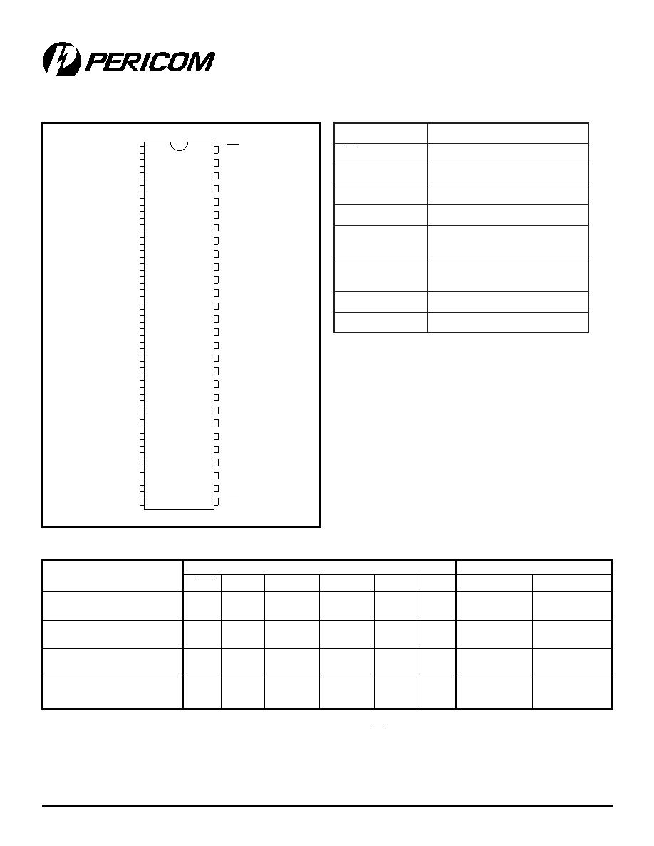
Product Pin Description
Truth Table(2)
Product Pin Configuration
e
m
a
N
n
i
Pn
o
it
p
i
r
c
s
e
D
E
O
x)
W
O
L
e
v
it
c
A
(
st
u
p
n
I
el
b
a
n
E
t
u
p
t
u
O
R
I
D
xl
o
rt
n
o
C
n
o
it
c
e
ri
D
A
B
K
L
C
x
,
B
A
K
L
C
xst
u
p
n
I
e
sl
u
P
k
c
o
l
C
A
B
S
x
,
B
A
S
xst
u
p
n
I
l
o
rt
n
o
C
t
c
el
e
S
x
A
x
st
u
p
n
I
A
r
e
t
si
g
e
R
a
t
a
D
st
u
p
t
u
O
B
r
e
t
si
g
e
R
a
t
a
D
x
B
x
st
u
p
n
I
B
r
e
t
si
g
e
R
a
t
a
D
st
u
p
t
u
O
A
r
e
t
si
g
e
R
a
t
a
D
N
Gd
n
u
o
r
G
V C
C
r
e
w
o
P
56-PIN
V56
A56
Inputs
Data I/O
Function
xOE
xDIR
xCLKAB xCLKBA
xSAB xSBA
xAx
xBx
Store A, B Unspecified (1)
XX
↑
X
Input
Unspecified(1)
Store B, A Unspecified (1)
XX
X
↑
X
Unspecified (1)
Input
Isolation
H
X
H or L
X
Input Disable
Store A and B Data
H
X
↑↑
X
Input
Real Time A Data to B Bus
L
H
X
L
X
Input
Output
Stored A Data to B Bus
L
H
H or L
X
H
X
Input
Output
Real Time B Data to A Bus
L
X
L
Output
Input
Stored B Data to A Bus
L
X
H or L
X
H
Output
Input
Note:
1. The data output functions may be enabled or disabled by various signals at the xOE or xDIR inputs. Data input functions are always
enabled, i.e., data at the bus pins will be stored on every LOW-to-HIGH transition on the clock inputs.
2. H = High Voltage Level
X = Don't Care
L = Low Voltage Level
↑ = LOW-to-HIGH Transition
发布紧急采购,3分钟左右您将得到回复。
相关PDF资料
PI74ALVCH16652A
IC 16-BIT BUS TXCVR/REG 56-TSSOP
PI74ALVCH16721A
IC 20-BIT FLIP-FLOP 56-TSSOP
PI74ALVCH16823A
IC 18-BIT INTERFACE-F/F 56-TSSOP
PI74ALVCHR162245AEX
IC TXRX 16BIT BIDIR 3ST 48TSSOP
PI74ALVTC16241A
IC BUFF DVR TRI-ST 16BIT 48TSSOP
PI74ALVTC16244K
IC BUFF DVR TRI-ST 16BIT 48TVSOP
PI74ALVTC16245A
IC 16-BIT BIDIR TXCVR 48-TSSOP
PI74ALVTC16373A
IC 16-BIT TRANSP LATCH 48-TSSOP
相关代理商/技术参数
PI74ALVCH16646V
制造商:未知厂家 制造商全称:未知厂家 功能描述:Dual 8-bit Bus Transceiver
PI74ALVCH16652
制造商:未知厂家 制造商全称:未知厂家 功能描述:Logic | 16-Bit Bus Transceiver w/Register
PI74ALVCH16652A
功能描述:IC 16-BIT BUS TXCVR/REG 56-TSSOP RoHS:否 类别:集成电路 (IC) >> 逻辑 - 缓冲器,驱动器,接收器,收发器 系列:74ALVCH 标准包装:1,000 系列:74ABT 逻辑类型:寄存收发器,非反相 元件数:1 每个元件的位元数:8 输出电流高,低:32mA,64mA 电源电压:4.5 V ~ 5.5 V 工作温度:-40°C ~ 85°C 安装类型:表面贴装 封装/外壳:24-SOIC(0.295",7.50mm 宽) 供应商设备封装:24-SOIC 包装:带卷 (TR)
PI74ALVCH16652V
制造商:未知厂家 制造商全称:未知厂家 功能描述:Dual 8-bit Bus Transceiver
PI74ALVCH16721
制造商:未知厂家 制造商全称:未知厂家 功能描述:Logic | 20-Bit Flip-Flop
PI74ALVCH16721A
功能描述:IC 20-BIT FLIP-FLOP 56-TSSOP RoHS:否 类别:集成电路 (IC) >> 逻辑 - 触发器 系列:74ALVCH 产品变化通告:Product Discontinuation 27/Jan/2012 标准包装:2,000 系列:74LCX 功能:标准 类型:D 型总线 输出类型:三态非反相 元件数:1 每个元件的位元数:8 频率 - 时钟:150MHz 延迟时间 - 传输:1.5ns 触发器类型:正边沿 输出电流高,低:24mA,24mA 电源电压:2 V ~ 3.6 V 工作温度:-40°C ~ 85°C 安装类型:表面贴装 封装/外壳:20-SOIC(0.209",5.30mm 宽) 包装:带卷 (TR) 其它名称:MC74LCX574MELG-NDMC74LCX574MELGOSTR
PI74ALVCH16721V
制造商:未知厂家 制造商全称:未知厂家 功能描述:20-Bit D-Type Flip-Flop
PI74ALVCH16820
制造商:未知厂家 制造商全称:未知厂家 功能描述:Logic | 10-Bit Flip-Flop w/Dual Outputs